
REPAIR LOGS
This is the place where I'll be sharing insights on repairs I've done, including pictures and video links!
Note: if you wish to hire me for a repair job, please see the bottom of the page for guidelines and contact.


05/18/2019
Sega Genesis Model 1
(aka Mega Drive is Mega Fried)
I've been on a mad spree lately
repairing every piece of Sega hardware I could get my hands on. I had an absolutely ravaged Sega Genesis that had been sitting in my closet for almost 10 years...
Spring cleaning ? You bet!
Even the best of us make mistakes,
and I am certainly no exception. Way back in 2010 I was "upgrading" a Genesis model 1 for S-video and overclocking. While finicking with the Motorola 68000 CPU I accidentally shorted out the clock signal :( *poof* there went the 68K and the 315-5487 ASIC!
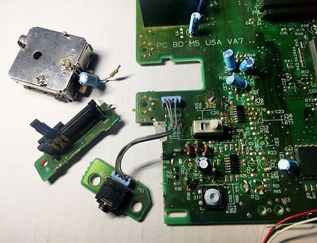
The mutilated audio stage with dissected RF modulator

Believing all was lost I tossed the poor beast into the bottom of my scrap bin. Over the next 9 years I harvested its organs piece by piece until little remained. I used its SRAM chips to repair a Neo Geo MV-1. I ripped out its RF circuitry to test signals to an RF-only CRT in 2016. I drilled out the volume slider. I harvested the LDO regulator. I ripped out the CXA1145 chroma encoder. I also pulled both audio omp amps. And as if that wasn't enough, I used to go in and pull all sorts of capacitors and resistors from it, too.
What was left of the video output stage, yikes!
Notice the pads for pins 2,3,4,5,6,7,11,13, and 22 are gone.
After leveling up my repair skills more recently I had the crazy notion of giving this another go. After all, I would learn in the process, right?
The first step was figuring out if the 315-5487 was truly fried. If it was, then this really would be pretty hopeless. I knew I had blown the 7.67Mhz oscillator, but what if I had only blown part of the chip, and not the whole thing...?

The 315-5487. Notice that the factory didn't use enough solder paste for the pins (see the exposed copper?) That became a problem for me later.
All the clock signals are derived from a master clock (53.69Mhz - NTSC) and divided down internally within the 315-5487 ASIC. This is the same for all Sega Genesis models. That internal clock is then used to produce other clock outputs including the subcarrier output which is responsible for the pixel clock and Z80 (SMS master clock). It also is responsible for creating the synchronization pulses used for video output (V, H, and C Sync respectively).

The Master clock taken from the Amstrad schematics using the same ASIC. For NTSC, a 53.69Mhz clock is used, not the PAL clock shown here.
My theory was this: even though I had blown the VCLK for the main CPU, perhaps it was only blown on the output side of the internal ASIC logic. If it is still divided internally, and the other clocks still work, I could actually feed in my own 7.67Mhz clock with a new 68K chip!
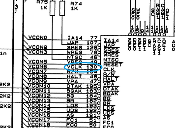
Pin 130 is what I killed :(

I replaced the SRAM, the 68K, cut the 7.67Mhz trace, injected my own clock (originally tested with a simple 10Mhz crystal, since I knew the Genesis could run games at that slight overclock frequency), plugged in a game cartridge and began poking around with my oscilloscope.
What did I find? The internals of the ASIC were still dividing down to 3.57Mhz and making the C Sync pulses! My theory was proving to be correct...
The final repair (hack) using an LTC1799 for the custom clock
The chip I used to create the custom 7.67Mhz CPU clock is the LTC1799 by Analog Devices. What is especially nice about this chip as it uses a simple resistor and a tri-state logic select pin to determine the output frequency, no programming required. >>>
Using the provided equation >>>
I found that an Rset of 13,030ohms with DIV set to ground gave me the needed output frequency.


After re-seating the dirty cartridge a few times I was finally able to read off video data from the ASIC R,G,B out pins (pins 35, 36, and 37) from my oscilloscope. >>>
I can't tell you how excited I was to see the video waveforms changing over time. It was alive!

Probe points for the R,G,B signals (under R12 silk)

Working video waveform (Green, in this case)

Fully functional 3.57Mhz clock waveform!
Now came the long and arduous process of repairing all the damaged analog output circuitry...
First up was the CXA1145 video encoder >>>
Amazingly, I never threw out the one stored in my parts bin for the last 9 years (!)
It was tricky finding all the missing cap values and repairing hidden cut traces and missing pads.

Replacing an SMD chip is one thing, but replacing and reconnected lots of damaged pads and traces is another...

Then, I replaced the RF modulator which was still somehow floating around in my scraps of electronic parts :)
This modulator has 3 input pins: composite video (CVBS), mono audio, and +5v (case is ground). That's why it's ideal for pulling out to test RF TVs!
Video encoder and RF modulator back in place
After successfully generating a composite video output it was time to tackle the audio...
Important note: the video encoder is responsible for creating a voltage reference used for the audio stage! (pin 14 of the CXA1145 is Vref) This had me chasing my tail a bit. It is also used to buffer the mono audio output (pins 8 and 9).
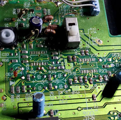
The lack of solder paste on the 315-5487 had created a poor connection between the FM audio power pin (pin 57) and the main PCB. This was definitely worsened by the board being flexed and thrown about my scrap bin over the years. (see 3rd image from the top)
Cleaning up after removing the old flux-soaked nasty "upgrade" opamps
Then came the opamps. Not only had I ripped up traces for the SOIC chips previously, I had cut some traces attempting my "upgrade" to a better opamp in 2010.
I also had removed almost every electrolytic capacitor and a bunch of SMD resistors. Fortunately I found a really nice board scan to help me along with the assistance of service manual schematics

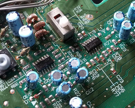
Ah, much better!
After that I needed to take this thing off my bench supply and replace the insulated TO-220 5V regulator. I also needed to replace various missing resistors and capacitors...
Fresh thermal paste! Just what a growing IC needs

The one last painful thing remaining was soldering back the volume slider that I had drilled out. It was rough repairing the cut out and bent PCB substrate. Even worse, I had to gently heat the slider plastic with a hot air gun because it had bent out of shape in the scrap bin! It was tricky getting it to align with the guide inside the shell of the outer case.
Sure enough though, it works great after 9 years of abuse. Genesis DOES!
Repairing the bent and sawed PCB was hard :(

The fully repaired PCB. Completely OEM condition now!
And here I am finally - about to play Sonic 2 in bed! >>>
Yes, it was a long and treacherous journey to repair a game console worth about $50. But I learned a ton of new things along the way and saved a life - a Sega Genesis life - from the landfill :)

[Stay tuned as I update this page with more technical docs for Sega repairs...]
Next repair up...
SEGA CDX
08/07/2017
Pioneer Laseractive
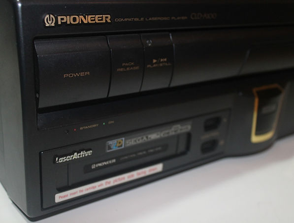
Every once in a while someone contacts me to fix something truly special. Something large, heavy, vintage, and worth hundreds in shipping charges.
This month it was a CLD-A100 Pioneer Laseractive (with Sega PAC). I had one of these gorgeous units back in the early 00's and it was a joy to see one again! This time around however, I went to put all my hardware knowledge to work so I could really understand this beast, or at least the Sega unit inside of it...
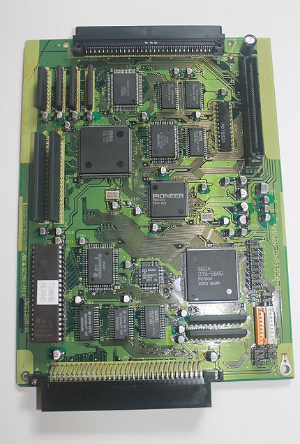

What is fascinating about the Laseractive is that it doesn't use any special advanced chipset to achieve these excellent results. In fact, it uses almost exactly the same chipset as the late model Genesis 2's, which are somewhat infamous for lackluster video and audio quality. This is mostly due to their use of the Fujitsu MB3514 video encoder: a knock-off of the Sony CXA1145 and the mediocre 315-5684 mixing opamp. However, power supply filtering issues are also largely the culprit as well as poor grounding techniques.
I used to think the 315-5660 was largely responsible too - after all, it has VRAM and the Yamaha audio chip built inside with the VDP, creating an understandable amount of interference. The Laseractive has the same chip though, and seems to not suffer from these ailments. It likely helps that the encoder itself is handled by Pioneer this time, and not dependent on the Sega ASIC for its FSC clock.

This unit would not boot Genesis games or enter the BIOS after a recap had been attempted by someone. Not only that, but the previous repair person fitted it with a CR2032 lithium battery. Sega CDs use rechargeable lithium batteries though, and the MB3790 could eventually blow up a CR2032 or cause it to leak by forcing current through it. It's now fitted with a proper LIR2032 rechargeable.
To get the system to boot required using a microscope and SMD tools to reflow some leaking electrolyte acid between pins as well as removing shorts around the Sega CD ASIC. These problems were very hard to spot and are the understandable byproduct of a decent recap gone awry.
For a more detailed run down, you can see my video posted online covering the repair. And for a complete .zip file of all the hires images plus other useful ones from around the web, click here.


Sega PAC under microscope showing leaking capacitor damage (2017)
My mod of the world's first 32X in a Laseractive, circa 2005


More Repairs Coming Soon!
In the meantime, check out all my repair videos online over here.
Repair Guidelines
I am very selective about which repairs I take on. If you are interested in hiring me to fix your vintage gear then the following are some things to keep in mind:
-
I don't take on jobs for <$100 labor (not including shipping costs)
-
Turnaround times are 1 month minimum (sometimes longer for parts ordering)
-
Customers are responsible for any damages incurred in transit. I suggest shipping insured.
-
If your order requires parts, then there will be a charge upfront. Most orders are requested to be paid in part prior to beginning work
-
In general, repairs are not "guaranteed." You are paying for my time, tools, and expertise in attempting a repair. That said, I have an excellent track record for the work I do and have references available.
-
Emails for work updates will be limited to a bi-weekly basis, though sometimes sooner if there are important questions.